Showing posts with label Misc. Circuits. Show all posts

Tuesday, July 19, 2011

Ultrasonic Position System

The ultrasonic position system uses ultrasonic transmitters/receivers to triangulate position of the robots used in GE423. Each of three transmitters uses a distinct frequencies: 23 kHz, 31 kHz, and 40 kHz. The 2812 DSP is used to measure signal timing and calculate position based on these values. The design of the electronics, as well as discussion of the software development is presented below.

The electronics were not intergrated with the 6713 DSP on the robot.
Note: To get around the issue of clock syncing, the robot will start in a known position, and calculate position for four cycles before proceeding. An alternative to this would be to add a fourth transmit frequency and use the 4th signal to sync the robot clock with the transmit clock.

1.0 Hardware

A wide variety of hardware was used for this project. The hardware was chosen based on availability and price. By no means is the solution presented "the best"or the only way to achieve the desired results, but it is a workable solution.

1.1 Ultrasonic Transmitters/Receivers

The ultrasonic sensor were purchased from Massa. The TR-89/B series where chosen because they come in 3 different frequencies, and they were stock parts. There is no pdf data sheet available on the Massa website, all information if available here. The main drawback of using Massa is there $500 minimum order, and the sensors aren't cheap at about ~$30 each.

1.2 Transmit Circuit

A schematic of the transmit circuit looks like:

Images of the perf-boarded transmit circuits:

Details on the components of the transmit circuit can be found in the subsection below:

1.2.1 Frequency Generation

The transmit circuit take from the Massa Website looks like:
Source:http://www.massa.com/datasheets/graphics/tr89_data.gif
Where R1 is a 10k 10 turn precision wound potentiometer, and U1 is a CD4039B NAND Schmitt Trigger. The tuning resistor R2 and L where left out to increase the transmit power around the base frequency. The potentiometer was adjusted until the frequency was the desired base frequency. A 1k resistor was added in parallel with the potentiometer to give a higher resolution. For the 40 kHz case, a smaller capacitor was required to reach the base frequency. Make sure to tune the circuit with the ultrasonic transducers attached, because the additional impedance will change the transmit frequency. The 12 Vdc was generated by a lab supply.
The output at point TP1, is a 12V peak to peak is a square wave at the desired frequency. The point TP1 was connected to the Driver Signal Circuit presented below.

1.2.2 555 Timer Circuit

The documentation for the 555 timer can be found here. An a picture of how it is wired can be 


seen below:
Source:http://www.williamson-labs.com/480_555.htm
Using the handy calculator for Ra, Rb, and C found here, Ra=100k ohm, Rb=200k ohm, and C=2.2 mircoF.

1.2.3 Driver Signal Circuit

The 35 Vdc supply is manufactured by Ultravolt, part number 1/4Aa24-P30. This supply is actually a 0-250 Vdc supply that uses a potentiometer to control voltage output.. The transistor used is an IRF520 n-channel MOSFET.

1.3 Receive Circuit

A block diagram of the receive circuit can be seen below:

And a picture of the perf-boarded receive circuit can be seen below:

Details on the components of the receive circuit can be found in the subsection below:


1.3.1 Low Signal Amp Circuit

An instrumentation amplifier made by Analog Devices was used to amplify the low signal output of the ultrasonic receivers. The actual part used was the AD620, one is recquired for each receive channel. Analog has a nice tool here, to size the gain resistor, Rg. Based on experiments, a gain value of 33 was chosen, resulting in a Rg of 1.5k ohm. The AD620 was wired as follows:
Source:http://www.analog.com/images/Product_Descriptions/3888333375812882340AD620_fbs.gif

1.3.2 Comparator Circuit

The analog comparitor used was part number LM339. The volatage divdier was powered using +5 Vdc to creat the digital level output signal. The output from each instrumentation amplifier was wired to the "+" terminal, and the "-" was wired to 3 volts. The 3 Vdc signal was created from the +15 Vdc supply using a voltage divider. The output of the comparitor was wired to a 5 Vdc via a 3k resistor.

2.0 Software

The timing of the hardware interrupts from the 2811 is calculated, and from the times, position is calculated in the 2D plane using a combination of least squared fit and Jacobian iteration.

2.1 Matlab Triangulation Code

The first algorithm was developed using Matlab. This code can be found here. The algorithm is not stable for all input parameters, a good set of test conditions are:
[x,y]=blah(.010,.012,.012)
[x,y]=blah(.009,.014,.012)
[x,y]=blah(.011,.011,.011)
Note the highly descriptive function named blah

2.2 DSP C Code

The c code for the 2812 DSP is in the attached zip file. The code works as following:
  1. Hardware interrupt pin get triggered
  2. Record absolute clock time when pin transition occurs
  3. Go back to step 1,and once all three pins have been triggered:
    1. (only do this step the first time through the code) Assume robot stationary, acquire base transmit period for each frequency by averaging first 4 values, this step syncs the clocks of the transmitters to the robot
    2. Calculate time from transmitter to robot for each frequency
    3. Triangulate position of robot using least squared fit to data points
    4. Wait for fixed amount of time, ignore hardware interrupts during this time because of the nature of the transmit signal
    5. Go back to Step 1

3.0 Lessons Learned

  1. A resistor was needed in parallel with the tuning potentiometer to give better resolution
  2. A resistor was required in parallel with the US transmitter for the circuit to function because the transmitter is like a capacitor.

4.0 Acknowledgments

Various people and online resources aided in this project:
  • GE423 Lab Instructor: Dan Block
  • GE423 TAs: Dave Johnson, Daniel Herring
  • My officemate: Steve Tschopp
  • Misc. Consultation: Tim Cargol
  • Misc Websites:
    • http://ourworld.compuserve.com/homepages/Bill_Bowden/555.htm
    • http://www.williamson-labs.com/480_555.htm
    • http://www.massa.com
    • http://www.digikey.com (source for datasheets)

Car Wireless Alarm Circuit Diagram

This FM radio-controlled anti- annexation anxiety can be acclimated with any agent accepting 6- to 12-volt DC accumulation system. The mini VHF, FM transmitter is adapted in the agent at night back it is anchored in the car balustrade or car park. The receiver assemblage with CXA1019, a distinct IC-based FM radio module, which is advisedly accessible in the bazaar at reasonable rate, is kept inside. Receiver is acquainted to the transmitter's frequency. Back the transmitter is on and the signals are actuality accustomed by FM radio receiver, no hissing babble is accessible at the achievement of receiver.


Appropriately transistor T2 (BC548) does not conduct. This after-effects in the broadcast disciplinarian transistor T3 accepting its advanced abject bent via 10k resistor R5 and the broadcast gets energised. Back an burglar tries to drive the car and takes it a few metres abroad from the car porch, the radio articulation amid the car (transmitter) and anxiety (receiver) is broken. As a aftereffect FM radio bore gene-rates hissing noise. Hissing AC signals are accompanying to broadcast switching circ- uit via audio transformer. These AC signals are rectified and filtered by diode D1 and capacitor C8, and the consistent absolute DC voltage provides a advanced bent to transistor T2.

Appropriately transistor T2 conducts, and it pulls the abject of broadcast disciplinarian transistor T3 to arena level. The broadcast appropriately gets de-activated and the anxiety affiliated via N/C contacts of broadcast is switched on. If, by chance, the burglar finds out about the wireless anxiety and disconnects the transmitter from battery, still alien anxiety charcoal activated because in the absence of signal, the receiver continues to aftermath hissing babble at its output. So the burglar anxiety is fool-proof and awful reliable.

Hot Water Level Indicator

Notes:
Save fuel bills and the economy of the planet with this circuit. SW1 is a normally open press button switch which allows you to view the level of hot water in a hot water tank. When pressed the voltage difference at the junction of the thermistor and preset is compared to the fixed voltage on the op-amps non-inverting input. Depending on the heat of the water in the tank, the thermistors resistance will toggle the op-amp output to swing to almost full voltage supply and light the appropriate LED.
Construction:
Masking tape was used to stick the bead thermistors to the tank. Wires were soldered and insulated at the thermistors ends. A plastic box was used to house the circuit. Battery life will probably be 4 to 5 years depending on how often you use the push switch, SW1.
Sensor Placement:
Thermistors NTC1-4 should be spread evenly over the height of the tank. I placed NTC1 roughly 4 inches from the top of my tank and the others were spaced evenly across the height of the hot water tank. As hot water rises the lowest sensor indicates the fullest height of hot water and should be about 8 to 10 inches from the bottom of the tank.
Calibration:
With a full tank of hot water adjust P1-4 so that all LED's are lit. As hot water rises, the sensor at the bottom of the tank will be the maximum level of hot water. "Hot" can be translated as 50C to 80C the presets P1-4 allow adjustment of this range.
Parts:
I have used a quad version of the LM324 but any quad opamp can be used or even four single op-amps.
R2-R5 I used 330ohm resistors, but value is not critical. Lower values give brighter LED output.
NTC1-4 The thermistors maximum resistance must roughly equal the resistance of the fixed resistor and preset. As negative temparature coefficient (NTC) thermistors are used, then their resistance decreases for increases in temperature. I used a thermistor from the Maplin Catalogue. Cold resistance was around 300K, hot resistance 15k. Alternative thermistors may be used with different resistance ranges, but the presets P1 to P4 must also be changed as well.
R7-10 series resistance, only required if your thermistors resistance is several ohms at the hottest temperature.
P1 - P4 Chosen to match the resistance of the thermistor when cold.
R1 & R6. These resistors are equal and bias the op-amp inverting input to half the supply voltage. I used 100k.

Water Level Indicator Alarm


This ambit not alone indicates the bulk of baptize present in the aerial catchbasin but additionally gives an anxiety back the catchbasin is full.
The ambit uses the broadly accessible CD4066, mutual about-face CMOS IC to announce the baptize akin through LEDs.
When the baptize is abandoned the affairs in the catchbasin are accessible circuited and the 180K resistors pulls the about-face low appropriately aperture the about-face and LEDs are OFF. As the baptize starts bushing up, aboriginal the wire in the catchbasin affiliated to S1 and the + accumulation are shorted by water. This closes the about-face S1 and turns the LED1 ON. As the baptize continues to ample the tank, the LEDs2 , 3 and 4 ablaze up gradually.
The no. of levels of adumbration can be added to 8 if 2 CD4066 ICs are acclimated in a agnate fashion.
When the baptize is full, the abject of the transistor BC148 is pulled aerial by the baptize and this saturates the transistor, axis the buzzer ON. The SPST about-face has to be opened to about-face the buzzer OFF.
Remember to about-face the about-face ON while pumping baptize contrarily the buzzer will not sound!

Sunday, March 27, 2011

Electronic mosquito repeller using CD4047


Description.
Here is the circuit diagram of an ultrasonic mosquito repeller.The circuit is based on the theory that insects like mosquito can be repelled by using sound frequencies in the ultrasonic (above 20KHz) range.The circuit is nothing but a PLL IC CMOS 4047 wired as an oscillator working at 22KHz.A complementary symmetry amplifier consisting of four transistor is used to amplify the sound.The piezo buzzer converts the output of amplifier to ultrasonic sound that can be heard by the insects.

Circuit diagram with Parts list.

Notes.
Assemble the circuit on a general purpose PCB.
The circuit can be powered from 12V DC.
The buzzer can be any general purpose piezo buzzer.
The IC1 must be mounted on a holder.

Electronic Mosquito Repeller Circuit


This circuit produces a tone above the human audible range and this is supposed to keep the mosquitoes away. You need a piezo diaphragm that will respond to 15kHz and these are very difficult to find. 

This electronic mosquito repellent schematic circuit diagram based on the 555 timer IC is a simple and useful mosquito repellent circuit . This mosquito repeller circuit generate an ultrasonic sound with a high output frequency that  allows spreading mosquitoes within a wide radius . The circuit is quite simple and require few external components . The oscillation frequency is given by the value of the R1, R2 and C1 components and can be modified changing the value of components or replacing the R2 fixed resistor with a variable resistor ( potentiometer ) .
The actual oscillation frequency of this electronic mosquito repeller circuit is around 45 KHz ( 46.5 KHz) so you need to use a good high frequency speaker , you can use a piezo speaker .

The circuit can be supplied from a 9 V DC power supply  . This repeller circuit can be used for almost any animal , it works on  : cats , dogs , rats  . Even if you don’t hear the sound generated by device don’t worry  because the high frequency is less audible by the human ear .

60W inverter using transistors


Description.
Here is the circuit diagram of a fully transistorized inverter that can drive up to 60W loads. Transistors Q1 and Q2 forms a 50Hz astable multivibrator. The output from the collector of Q2 is connected to the input of the Darlington pair formed by Q3 and Q4.Similarly the output of Q1 is coupled to the input of the pair Q5 and Q6. The output from the Darlington pairs drive the final output transistors Q7 and Q8 which are wired in the push pull configuration to drive the output transformer.
Circuit diagram.


Notes.
The circuit can be assembled on a vero board.
T1 can be a 230V primary to 9-0-9V, 6A secondary transformer.
Transistors Q4, Q6, Q7 and Q8 must be fitted with heat sinks.
Use a 12V, 7Ah battery for powering the inverter.
Slight adjustments can be made on the value of R3 and R4 to get exact 50Hz output.

Simple 100W inverter circuit


Description.
Here is the circuit diagram of a simple 100 watt inverter using IC CD4047 and MOSFET IRF540. The circuit is simple low cost and can be even assembled on a veroboard.

CD 4047 is a low power CMOS astable/monostable multivibrator IC. Here it is wired as an astable multivibrator producing two pulse  trains of 0.01s which are 180 degree out of phase at the pins 10 and 11 of the IC. Pin 10 is connected to the gate of Q1 and pin 11 is connected to the gate of Q2. Resistors R3 and R4 prevents the loading of the IC by the respective MOSFETs. When pin 10 is high Q1 conducts and  current flows through the upper half of the transformer primary which accounts for the positive half of the output AC voltage. When pin 11 is high Q2 conducts and  current flows through the lower half of the transformer primary in opposite direction and it accounts for the negative half of the output AC voltage.

Circuit diagram.
Notes.
B1 can be  a 12V/ 6Ah lead acid battery.
Q1 and Q2 must be fitted to a proper heat sink.
T1 can be a 9-0-9 V primary, 230V secondary, 150VA transformer .
Do not expect much from this circuit. The is very simple one suitable for low grade applications.

How to make an Inverter- Simple 40 Watt Inverter


How to make an Inverter

Description:This is the schematic of a simple 40W , 12 volts to 220 Volts inverter.You don’t believe, this is simple and cheap and working for me for last 4 years.The heart of the circuit is a CD 4047 IC which is wired as an astable multi vibrator here.Resistance and Capacitance at pin 1&2 determines the out put frequency.Here it is set to 60Hz.Due to this a two 180 degree out of phase ,120 Hz , 50% duty cycle waveforms will appear at pin 10 & 11.These waves are amplified by the complementary symmetry amplifier made of transistors BC 337 & TIP 3055 to drive the out put transformer.Don’t get feared of the technical terms, just wire it on a all purpose PCB.It is simple and will work.Don’t worry about the transformer windings ,buy a 220-110-0 primary,12-0-12 secondary , <50W transformer.You can select output voltage of 110V or 220V by a two way switch using such a transformer.Don’t worry if you don’t have such a transformer, a simple 220 to 12-0-12 will also do the trick sacrificing the 110V option or vice versa.The best way to get a transformer is to break all useless electronic devices in your trash.Most probably you will find the transformer or more components needed here!

Simple Inverter Circuit Diagram:


Tips : First wire to oscillator part only.Then check out put Pin 10 &11 of CD4047 to obtain the required wave forms ( two 120Hz ,180 degree out of phase,50% duty cycle waves. Then connect transistors ,transformer and load (25 W bulb for test).See it working!.

555 Timer IC Pin configuration


The 555 Timer IC is available as an 8-pin metal can, an 8-pin mini DIP (dual-in-package) or a 14-pin DIP.
This IC consists of 23 transistors, 2 diodes and 16 resistors. The explanation of terminals coming out of the 555 timer IC is as follows. The pin number used in the following discussion refers to the 8-pin DIP and 8-pin metal can packages.


Pin 1: Grounded Terminal. All the voltages are meas­ured with respect to this terminal.
Pin 2: Trigger Terminal. This pin is an inverting input to a comparator that is responsible for transition of flip-flop from set to reset. The output of the timer depends on the amplitude of the external trigger pulse applied to this pin.
Pin 3: Output Terminal. Output of the timer is avail­able at this pin. There are two ways in which a load can be connected to the output terminal either between pin 3 and ground pin (pin 1) or between pin 3 and supply pin (pin 8). The load connected between pin 3 and ground
supply pin is called the normally on load and that connected between pin 3 and ground pin is called the normally off load.
Pin 4: Reset Terminal. To disable or reset the timer a negative pulse is applied to this pin due to which it is referred to as reset terminal. When this pin is not to be used for reset purpose, it should be connected to + VCC to avoid any possibility of false triggering.
Pin 5: Control Voltage Terminal. The function of this terminal is to control the threshold and trigger levels. Thus either the external voltage or a pot connected to this pin determines the pulse width of the output waveform. The external voltage applied to this pin can also be used to modulate the output waveform. When this pin is not used, it should be connected to ground through a 0.01 micro Farad to avoid any noise problem.
Pin 6: Threshold Terminal. This is the non-inverting input terminal of comparator 1, which compares the voltage applied to the terminal with a reference voltage of 2/3 VCC. The amplitude of voltage applied to this terminal is responsible for the set state of flip-flop.
Pin 7 : Discharge Terminal. This pin is connected internally to the collector of transistor and mostly a capacitor is connected between this terminal and ground. It is called discharge terminal because when transistor saturates, capacitor discharges through the transistor. When the transistor is cut-off, the capacitor charges at a rate determined by the external resistor and capacitor.
Pin 8: Supply Terminal. A supply voltage of + 5 V to + 18 V is applied to this terminal with respect to ground (pin 1).

USB Battery Charger controller circuit using LM3622

From USB Battery Charger controller circuit using LM3622

Saturday, March 26, 2011

555 timer calculator (monostable and astable operation)

This 555 timer IC calculator can calculate frequency, duty cycle, and high and low output of timer IC operation on both monostable and Astable. This Calculator script was written by Robert Davis of Goldsmith College
555 timer IC
555 timer Pin number and designation:
pin 1- ground or common pin
pin 2- trigger pin
pin 3- output pin
pin 4- reset pin
pin 5- control pin
pin 6- threshold  pin
pin 7- discharge pin
pin 8- positive supply


555 MONOSTABLE OPERATION
Acts as one shot  pulse generator of output high duration of  T=RC ln(3)


555 timer monostable


R:


C:


T Output High (Seconds) =


555 TIMER ASTABLE OPERATION
555 timer astable operation


This operation has an output of continuous pulses of specified frequency and and duty-cycle.


R1:


R2:


C:


T1 Output High (Seconds) =

T2 Output Low (Seconds) =


T Total Period (Seconds) =


Frequency (Hz) =


Duty (%High) =

Simple LED Emergency Light Circuit


This LED emergency light project is simple, cheap and easy to build. The circuit do the charging of the battery and when the main source is not available such as in brownouts, the white LEDs automatically turn on. 
Initially, the voltage output  from 220V to 12V converter is fed to the input of LM317 regulator. Then this voltage is regulated down to 7.37V using 240 ohms and 1.2K resistor combination (see LM317 Calculator).
At this instant, the battery is in charging mode and the transistor Q1 is off. Indicator LED serves two purpose, one primarily is to give us idea that the battery is charging and another is to ensure that the Q1 is off.
During brownouts, the transistor Q1 is on and delivers current to 16 white LED of about 20mA each, thus a fully charged battery (6V/4.5Ah) can last up to 14 hours.

The charger has no built in over-current control but still it protects the battery from overcharging since the charging voltage is set only to 7.4V.


Project materials:
1pc - transformer - 220V to 12V-0-12V , center tap 12VA
16pc - 120 ohms resistor 1/4 W
16pc - white LED min 3V@30mA
1pc - red LED
1pc - 1000uF/25V electrolytic capacitor
3pc - 1N4001 diode
1pc - LM317 regulator
1pc - 1.5K resistor 1/4W
1pc - 240 ohms resistor 1/4W
1pc - 1.2k resistor 1/4W
1pc - 9012 pnp transistor or any of much higher capacity
1pc - 6V 4.5ah battery

Automatic LED Emergency Light


Description
This is the circuit diagram of a low cost emergency light based on white LED.The white LED provide very bright light which turns on when the mains supply is not there.The circuit has an automatic charger which stops charging when the battery is fully charged.

The IC LM 317 produces a regulated 7 V for the charging of Battery.Transistor BD 140 drives the out put.Transistor BC 548 and Zener diode controls the charging of the battery.

Tips
It is always better to connect a heat sink with BD 140.Before using the circuit out put of LM317 must be set to 7V by adjusting the potentiometer.

Wednesday, March 23, 2011

4069 Latching Relay Driver


Uses of Optoisolators

Consist of an LED (usually Infra-red) and a phototransistor close-coupled in a DIL IC package. Commonly used to isolate two sections of a circuit for safety reasons.

An example where you want to swap your case power or drive activity LED for something with a bit more bling, without endangering the motherboard. The optoisolator diode is connected in place of the case LED.


Non-Latching (Momentary) Switches.


The most common are push-button, but toggle switches too may be spring-loaded to return to one position after activating. In the catalogues, an (ON)-OFF description means it's only ON while you're holding the lever in place. With push-button, they're more often described as 'momentary-on' (push to make) or 'momentary-off' (push to break).

Here's how the two types could be used together to control ON-OFF action by latching a relay, a very common system on industrial control gear.

Relay Latching Circuit

The relay needs to have two or more poles (the switches) which can be change-over (double-throw) or single-throw types. 

The "On" switch S2 is a push-to-make (momentary on) type, and allows power through to the relay coil when pressed. This becomes an electro-magnet and pulls all the relay switches over to the 'no' (normally-open) position. (With relays, 'normally-open' and 'normally-closed' refer to the switch positions with no power applied to the coil.)

Relay switch Sw2 now keeps power running to the relay coil after the "On" button has been released, latching the relay into the 'on' position.

Relay switch Sw1 is used to switch power to whatever load you have attached, (Extra relay switches would be used, for example, to control a 3-phase electric motor.)

Pressing the "Off" button S1, a push-to-break (momentary off) type, breaks the power circuit, deactivating the relay electro-magnet and sending its switches back to the 'nc' (normally-closed) position.

The diode D1 gives an easy path to any voltage spike produced when the relay coil turns off (back-EMF) protecting any sensitive equipment on the same circuit.

Friday, March 11, 2011

Logic gate symbols


There are two series of symbols for logic gates:

  • The traditional symbols have distinctive shapes making them easy to recognise so they are widely used in industry and education.
    AND gateNOR gateNOT gate
  • The IEC (International Electrotechnical Commission) symbols are rectangles with a symbol inside to show the gate function. They are rarely used despite their official status, but you may need to know them for an examination.
    AND gateNOR gateNOT gate

Inputs and outputs

AND gate with inputs and output labelled
Gates have two or more inputs, except a NOT gate which has only one input. All gates have only one output. Usually the letters A, B, C and so on are used to label inputs, and Q is used to label the output. On this page the inputs are shown on the left and the output on the right. 


The inverting circle (o)

Some gate symbols have a circle on their output which means that their function includes inverting of the output. It is equivalent to feeding the output through a NOT gate. For example the NAND (Not AND) gate symbol shown on the right is the same as an AND gate symbol but with the addition of an inverting circle on the output. 

All Gates Pinouts


Hex Three State Buffer
Quad AND Gate
Four Line to 16 Line DeMultiplexer
Hex Inverter
Eight Line to One Line Multiplexer
Quad NAND Gate
Quad NOR Gate
Quad Operational Amplifier


Quad OR Gate

TTL NAND and AND gates


TTL gate

Transistor–transistor logic – Wikipedia, the free encyclopedia
The magnitude of this current is about 1.1 mA for a standard TTL gate and does not depend on the number of the parallel connected inputs (base-emitter junctions) belonging to one IC. The input source has to be low-resistive enough (< 800 Ω) so that the flowing current creates only a negligible ...
History - Theory - Packaging - Comparison with other logic ...
en.wikipedia.org/wiki/Transistor–transistor_logic

Logic family - Wikipedia, the free encyclopedia
Since the transistors of a standard TTL gate are saturated switches, minority carrier storage time in each junction limits the switching speed of the device. Variations on the basic TTL design are intended to reduce these effects and improve speed, power consumption, or both. The German ...
en.wikipedia.org/wiki/Logic_family

TTL logic gates This worksheet and all related files are licensed ...
For a true TTL gate (not high-speed CMOS), what is the default logic state of an input line that is left. floating (neither connected to VCC nor Ground)? Explain ...
What is the typical range of supply voltages for a true TTL gate, and why can't this type. of logic gate operate from a wider range of voltages as ...
IOL is typically much greater than IOH for a TTL gate with totem-pole output circuitry. The reason. for this should be obvious from inspection of ...

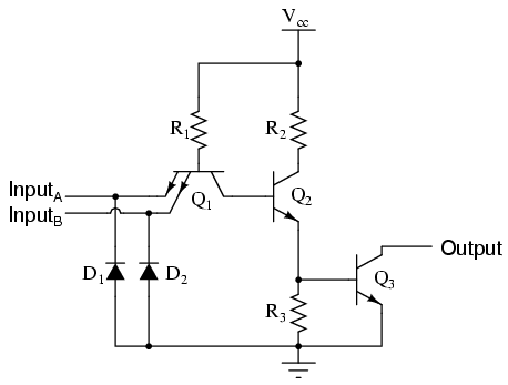
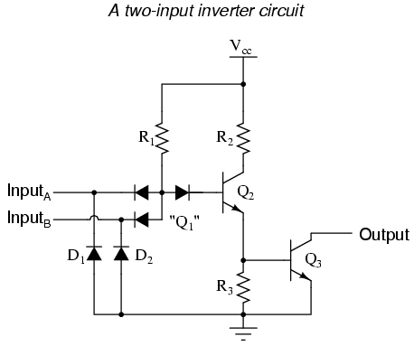
Suppose we altered our basic open-collector inverter circuit, adding a second input terminal just like the first:

This schematic illustrates a real circuit, but it isn’t called a “two-input inverter.” Through analysis we will discover what this circuit’s logic function is and correspondingly what it should be designated as.
Just as in the case of the inverter and buffer, the “steering” diode cluster marked “Q1” is actually formed like a transistor, even though it isn’t used in any amplifying capacity. Unfortunately, a simple NPN transistor structure is inadequate to simulate the three PN junctions necessary in this diode network, so a different transistor (and symbol) is needed. This transistor has one collector, one base, and twoemitters, and in the circuit it looks like this:
In the single-input (inverter) circuit, grounding the input resulted in an output that assumed the “high” (1) state. In the case of the open-collector output configuration, this “high” state was simply “floating.” Allowing the input to float (or be connected to Vcc) resulted in the output becoming grounded, which is the “low” or 0 state. Thus, a 1 in resulted in a 0 out, and vice versa.
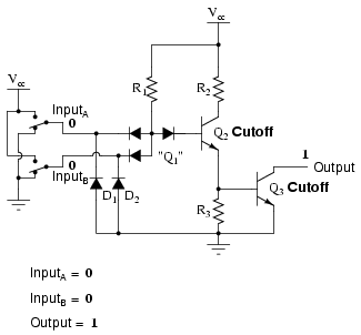
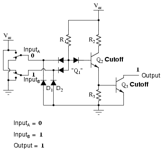
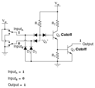
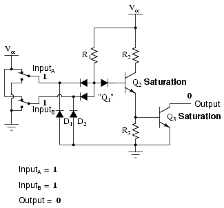
Since this circuit bears so much resemblance to the simple inverter circuit, the only difference being a second input terminal connected in the same way to the base of transistor Q2, we can say that each of the inputs will have the same effect on the output. Namely, if either of the inputs are grounded, transistor Q2 will be forced into a condition of cutoff, thus turning Q3 off and floating the output (output goes “high”). The following series of illustrations shows this for three input states (00, 01, and 10):
In any case where there is a grounded (“low”) input, the output is guaranteed to be floating (“high”). Conversely, the only time the output will ever go “low” is if transistor Q3 turns on, which means transistor Q2 must be turned on (saturated), which means neither input can be diverting R1 current away from the base of Q2. The only condition that will satisfy this requirement is when both inputs are “high” (1):
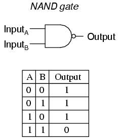
Collecting and tabulating these results into a truth table, we see that the pattern matches that of the NAND gate:
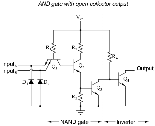
In the earlier section on NAND gates, this type of gate was created by taking an AND gate and increasing its complexity by adding an inverter (NOT gate) to the output. However, when we examine this circuit, we see that the NAND function is actually the simplest, most natural mode of operation for this TTL design. To create an AND function using TTL circuitry, we need to increase the complexity of this circuit by adding an inverter stage to the output, just like we had to add an additional transistor stage to the TTL inverter circuit to turn it into a buffer:
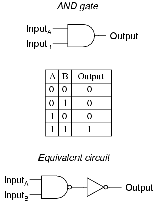
The truth table and equivalent gate circuit (an inverted-output NAND gate) are shown here:
Of course, both NAND and AND gate circuits may be designed with totem-pole output stages rather than open-collector. I am opting to show the open-collector versions for the sake of simplicity.
  • REVIEW:
  • A TTL NAND gate can be made by taking a TTL inverter circuit and adding another input.
  • An AND gate my be created by adding an inverter stage to the output of the NAND gate circuit.

TTL NOR and OR gates

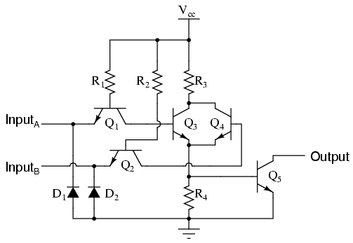
Let’s examine the following TTL circuit and analyze its operation:
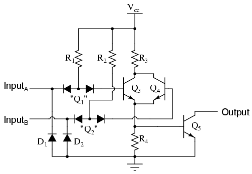
Transistors Q1 and Q2 are both arranged in the same manner that we’ve seen for transistor Q1 in all the other TTL circuits. Rather than functioning as amplifiers, Q1 and Q2 are both being used as two-diode “steering” networks. We may replace Q1 and Q2 with diode sets to help illustrate:
If input A is left floating (or connected to Vcc), current will go through the base of transistor Q3, saturating it. If input A is grounded, that current is diverted away from Q3‘s base through the left steering diode of “Q1,” thus forcing Q3 into cutoff. The same can be said for input B and transistor Q4: the logic level of input B determines Q4‘s conduction: either saturated or cutoff.
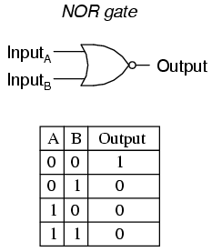
Notice how transistors Q3 and Q4 are paralleled at their collector and emitter terminals. In essence, these two transistors are acting as paralleled switches, allowing current through resistors R3 and R4 according to the logic levels of inputs A and B. If any input is at a “high” (1) level, then at least one of the two transistors (Q3 and/or Q4) will be saturated, allowing current through resistors R3 and R4, and turning on the final output transistor Q5 for a “low” (0) logic level output. The only way the output of this circuit can ever assume a “high” (1) state is if both Q3 and Q4 are cutoff, which means both inputs would have to be grounded, or “low” (0).
This circuit’s truth table, then, is equivalent to that of the NOR gate:
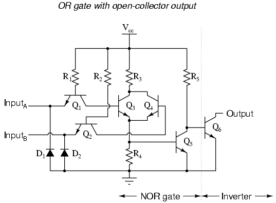
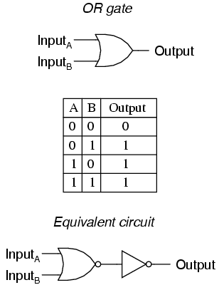
In order to turn this NOR gate circuit into an OR gate, we would have to invert the output logic level with another transistor stage, just like we did with the NAND-to-AND gate example:
The truth table and equivalent gate circuit (an inverted-output NOR gate) are shown here:
Of course, totem-pole output stages are also possible in both NOR and OR TTL logic circuits.
  • REVIEW:
  • An OR gate may be created by adding an inverter stage to the output of the NOR gate circuit.